Logic gates are used to make combinational logic. Now, we are going to move on to sequential logic.
Combinational Logic
- Output depends entirely upon input
- Output is always the same for same input(logically consistent)
- There is no sense of “memory”
Sequential Logic
- Output depends upon input as well as previous output
- Output may not be the same as the last output even if inputs are the same
- There is a sense of “memory”
Sequential takes the output of the device and puts it back into the input of the device. This is called a feedback path. It is the basis of memory in the CPU.
The RS Latch

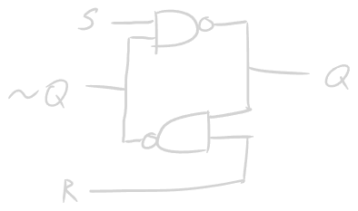
This is the R-S latch, the most fundamental unit for static memory. Notice how the output to Q gets fed back into the input. This has the ability to “store” its last output(or “latch” onto incoming data). There are two inputs and two outputs:
- S -> SET
- R -> RESET
- Q -> OUTPUT
- ~Q -> NOT(Q) (Also an output)
This is an example of a bi-stable circuit. This means it can exist in two stable states. Those states can be set with the S-R signals. These logical states are maintained through the feedback paths.
R-S Latch Truth Table
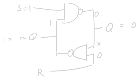
To start, lets set a known state of S=1, R=0.

This is what we get through the first iteration of the latch. We want to begin with the bottom NAND gate, because even if we don’t know the value of the feedback path(denoted X), we can still figure out its output. From there, we can construct the rest of the loop for the full iteration. Notice that after all the values have been set, at this input configuration, the value of the outputs as well as the feedback path all stay the same.
Since the input combinations are essentially performing “actions” on the known state of the feedback path/output, we denote the input combinations “actions”. This input combination is called a RESET. This is because, as we saw, no matter what the previous state was, we can get to a known state by performing it. We can make a truth table for these actions.
| ACTION | S | R | Q | ~Q |
|---|---|---|---|---|
| ILLEGAL | 0 | 0 | 1 | 1 |
| SET | 0 | 1 | 1 | 0 |
| RESET | 1 | 0 | 0 | 1 |
| HOLD | 1 | 1 | Q | ~Q |
Using the same method, we can find another output. The SET action is another action that takes us from an unknown state to a known state. Notice that RESET takes the output Q to 0, while SET takes it to 1.
Next, we need to look at a conditional action, one that depends on the current state. This is the HOLD action, which will make the last output stay in the feedback path. We denote the value in the truth table as Q and ~Q, because their values are also based on the last state of both these outputs. Finally, we have an illegal action, which is when both inputs are 0.
The Gated D-Latch
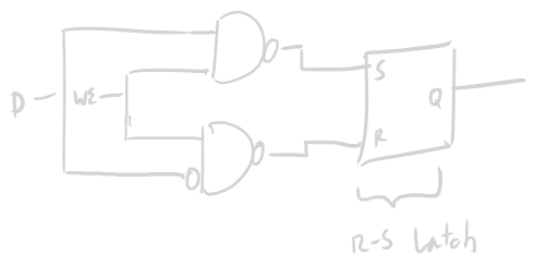
The Gated D-Latch is an improvement upon the R-S Latch that manages the illegal state you could call on it by setting S=0, R=0.

This is the Gated D-Latch. It has two inputs that feed into the S and R inputs from the R-S Latch. Q and ~Q are still valid outputs. ~Q is simply omitted.
- D -> DATA
- WE -> Write Enable
Truth Table
We can follow the same process as the R-S latch to find known states and create a truth table.
| ACTION | WE | D | Q |
|---|---|---|---|
| OPEN | 1 | D | D |
| CLOSED | 0 | X | Q |
- The OPEN action essentially has Write Enable set to open, and then sets the output to whatever the data is. The output is D, which means that as long as WE=1, the output Q as well as the feedback path will be set to D
- On the other hand, the CLOSED action will call the HOLD function on the R-S latch no matter what is put into the input by D(which is why we denote it X). Q will remain Q
As you can see, truth tables are difficult to use when representing sequential logical gates. This is because outputs are no longer a function of only the inputs. There is a notion of “Time dependence”.
Timing Diagram
![[Pasted image 20240207220250.png]]
This is what is known as a D-Latch timing diagram. It is essentially a graphical version of the truth table for a sequential logic gate. It shows how the inputs might change with time, and how the outputs will change as a result. The X axis is meant to represent time, and the Y axis is the input or output(HIGH=1, LOW=0).
Looking at timeslots 1 and 3, we see that WE=1. This means the device is open. This tells us that the Q output should follow whatever value the D input has, which it does. However, in timeslot 2, WE gets set to 0, which closes the input. This makes the Q output hold onto whatever was last set and stored, and isn’t affected by changed in D, which we can see it follows.
There is a slight delay between the change in the inputs and the change in the outputs. That is called the propagation delay. That is the time it takes to go through the gates, which is never instantaneous.
D-Flip-Flop Structure
This flip flop structure is very complex but very useful. It follows a configuration known as the Leader-Follower configuration(formerly known as master-slave).
![[Pasted image 20240207223536.png]]
This is the D-Flip-Flop. It consists of two D-latches joined together, with both the WE inputs connected via a CLOCK input, and an inverter on the left D-latch WE. Notice we only have one DATA input, and one output Q. Note that since the signals going to the WE terminals on the D-latches are always going to be opposite, one’s write will always be enabled, while the other will always be disabled.
As WE is changed, following its title, the latches will flip/flop back and forth between being opened and closed, always staying opposite one other. With respect to the configuration, the first latch is called the leader, and the second latch is called the follower. This is because the follower receives its input from only the leader latch.
Thinking of the OPEN and CLOSED commands, imagine the two D-latches like gates. By putting a clock that is inverted, we have made it so that the data cannot pass through all at once, since one gate will always be closed. Each data signal must wait for both a 0 signal and a 1 signal through the clock in its lifespan to be let through.
The effect of this is that the Flip-Flop only accepts new data when the CLK transitions from 0 to 1. This is referred as an edge triggered device. This means that the data transfer happens only when the clock is changing, rather than when the clock is in a state. The reason we use this is because it lengthens the window of opportunity to read from the flipflop but it shortens the window of opportunity to write.
A clock is simply a device that returns an oscillating signal at a certain frequency(Hz). The period is the length of one cycle of this clock, and the frequency is how many cycles it completes per second. Therefore, the period and frequency are inversely related
Registers
A D-latch register is a collection of D-latches controlled by a common WE signal. With an n-size register, we can store n bits. On the other hand, we also have a D-flip-flop register, which is the same concept with a collection of D-flip-flops. Both of these devices act the same as their individual counterparts(as long as the same clock signal is used for all of them), but are able to store larger amounts of data.
Finite State Machines
![[Pasted image 20240212153717.png]]
This circuit combines an incrementer with a D-flip-flop register that pulses at the rate of the clock. Assuming we start the D-flip-flop at zero, this circuit will count the number of pulses we receive from the clock.
This is an example of a finite state machine. A state machine consists of three parts:
- A register that stores the state
- A logic block that computes the next state given the current state and any inputs
- A logic block that computes the output based on the current state
![[Pasted image 20240212154124.png]]
Computer Memory
Computer memory is like a 2 x n table, in which each data entry has an ADDRESS and DATA. To look up data, we have to request the correct address. The number of locations that exist in our memory is called the address space. This is usually a power of 2. The number of bits we can store in a single data drawer(at a single address) is called the addressability.
The ideal memory interface has two basic operations: selecting an address to read, and selecting an address to write. There are standardized signals for these operations:
- A - address(n bits for a 2n address space)
- Dout - Contents of selected location during read
- Din - Contents we want to write to A
- WE - Write enable, determines which operation we are using Our memory would look like this:
![[Module 4 Notes 2024-02-12 15.54.54.excalidraw]]
It is preferable to build memory using flip-flops over latches.
Creating the read function for memory is simple. Since the address is a bitwise number representing the flip-flop who’s data we want, we can simply pass them through a MUX and get our output.
Creating the write function is a little more complicated. We will need a new logic device called the decoder. ![[Pasted image 20240212161616.png]]
This circuit is almost like a reverse-PLA or a reverse MUX. It turns the corresponding wire to 1 if and only if the number AB corresponds to it. This also implies that it only turns on a single wire at a time. This is exactly what we need for our WE input.
However, currently our D-flip-flops do not have WE lines, they only have clock lines. Therefore, we will still need to have the clock connected. However, on certain ticks, we want the flip flop to ignore the clock and keep its data. To do this, we will simply wire a MUX to the data line with the WE being the selector. For the 1 terminal, we will have our original data signal. However, on the 0 terminal, we will wire the output of the flip-flop. This will make it so the flip-flop will write its own data into itself when the WE is 0.
![[Pasted image 20240212162121.png]]
Usually this circuit is truncated:
![[Module 4 Notes 2024-02-12 16.22.23.excalidraw]]
Using all these concepts, our final memory module will look like this: ![[Pasted image 20240212162618.png]]
Some things to note:
- The WE signal is a global write enable signal, therefore we combine it with the output of the decoder. Therefore, if WE is 1, only one of the flip-flops will have a local WE of 1. If WE is 0, none of the flip-flops will have a local WE of 1(they will all be 0)
- One limitation of this design is you can only read or write at once, determined by the WE signal
When it comes to that last limitation of either being able to read or write at once, we can actually create an improved design that is able to write to one address while reading from another address at a time. This can be done very simply: add another signal for the address of where to write to. This creates independent read/write addresses, and allows us to perform these functions independently.
![[Pasted image 20240212163412.png]]
Another realization is that the read functions are actually independent of one other. Therefore, the MUX at the end can be multiplied with its own separate read address line and data output line, making it possible to read two, three, or any amount of flip flops at a time.
RAM and Memory Types
Real memory is usually denser and relies on some analog properties. However, there are two main kinds of RAM(Random Access Memory):
- Static RAM(SRAM)
- 6 transistors per bit
- Fast and maintains data as long as power is applied
- Dynamic RAM(DRAM)
- 1 transistor per bit
- Denser but slower
- Needs a capacitor to store information
- Takes more time to “charge” the storage element
Computer Memory Hierarchy
When computers are built, we allocate SRAM and DRAM based on their use cases. A CPU is fast, and requires a bit of memory called the register file, so we allocate that with SRAM. There is also more CPU-accessible memory outside the CPU itself called the cache. It is many cycles slower than the CPU, but it has megabytes of storage. Then, we have the main memory, or the RAM. This has storage in gigabytes, but its access is much slower(tens of clock cycles). Finally, for permanent memory that doesn’t lose its data when the power is removed, we have the disk. This has storage in terabytes, but is the slowest memory with access times in 1000s of ticks.